The Basics of Tenting
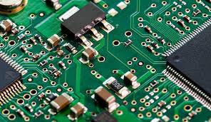
PCB Manufacturing Tenting in PCB manufacturing refers to covering the via holes with a solder mask to protect them from the elements, and prevent solder bridges from connecting to them during the assembly process. Vias are small holes that allow electric connection between different layers of a PCB. Leaving these vias unprotected allows contamination to collect and solder bridges are risked as well. Tenting is primarily a form of dry film solder mask that is applied over the vias before the soldering process, forming a 'tent' like cover.
Benefits of Tenting Vias
Tenting Vias - Reliability is the primary reason for tenting a via on a PCB. Tenting protects vias from environmental exposure, so that the via holes are not corroded or otherwise damaged. This is especially important in environments such as high-humidity or with corrosive chemicals that the PCB is in. In addition, tenting keeps the PCB structurally sound by not allowing any extraneous objects into the via and causing an electrical failure.
Materials and Techniques
What type of material used for the tenting will directly dictate how effective the process will be. Most often made of LPI (Liquid Photo-Imageable) solder mask or dry film solder mask. Leave-behind LPI is a matter of applying a liquid mask, cured by UV, that seals the vias most effectively and is long-term durable. The preferred method is known for its accuracy and uniform dispersion. Alternatively, a dry film solder mask is where a pre-formed film is carefully rolled over the entire / defined area, then exposed and developed to show a specific pattern. This is especially effective in some of the most complex PCB designs.
PAU against Other Via Protection Solutions
Tenting being a common option, there are other methods like plugging and capping in rendering other possible via protection map. Plugging is where the via holes are filled with an epoxy or soldermask material, capping is a subsequent process of applying a thin copper layer over the filled via. Tenting is much cheaper and more simple in comparison to these techniques and is generally the preferred option in high-volume manufacturing scenarios where reducing the number of additional processing steps can translate to large costs savings.
Use Cases & Industry Adoption
Tenting is extensively used in industries in which PCBs are subjected to harsh environments. From automotive to aerospace and consumer electronics, long-term reliability and longevity are critical. In these applications, it is critical to safeguard sensitive vias from potential impacts and in the event of their use, devices must perform reliably over the entire lifecycle.
For further details concerning tenting significance in PCB fabrication, we will be having an in-depth discussion.
Highlights Tenting is an imperative step in PCB manufacturer which protects via holes from harm which ensures the quality of the circuit boards and increases their lifespan. Manufacturers have recognized the importance of tenting over the past ten years, developing solutions for perfect application and the right usage of materials (such as thermoset webs), working to protect the board from the many environmental and mechanical stresses it will face to meet the high demands of today's new electronic devices.